Interfacing UART with DE0 Nano FPGA
Introduction:
Universal Asynchronous Receiver-Transmitter (UART) is one of the simplest and oldest forms of device-to-device digital communication. UART is a serial communication protocol that performs parallel to serial data conversion at the transmitter side and serial to parallel data conversion at the receiver side.
UART transmitter and receiver works asynchronously, which means there is no clock signal to synchronize the output of bits from the transmitting UART to the sampling of bits by the receiving UART. Instead of a clock signal, the transmitting UART adds Start and Stop Bits to the Data Packet being transferred. These bits define the beginning and end of the Data Packet so the receiving UART knows when to start reading the bits. When the receiving UART detects a Start Bit, it starts to read the incoming bits at a specific frequency known as the baud rate.
More on UART
One UART device consists of two parts : the first is Transmitter and the other is Receiver. It consists of two lines for data transmission, RX and TX, one in each direction as shown in the below figure. 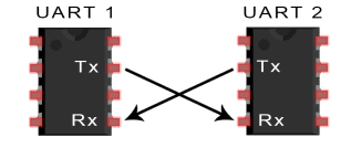 The UART devices receive and transmit the data in serial manner. The communication takes place in a particular data format i.e the data is sent and received in a Data Packet. Each Data Packet consists of a Start Bit followed by Data Bits (usually 5 to 9-bits long) and then Parity Bit and at the end is the Stop Bit. The figure below shows the structure of the Data Packet used in UART communication.
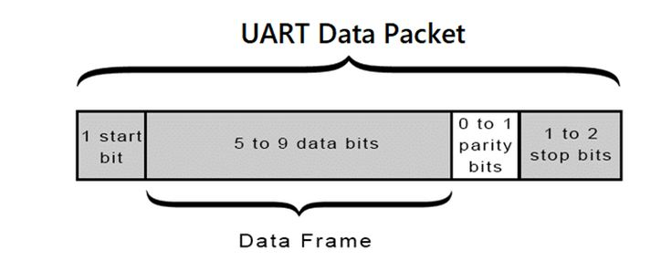
- Start Bit
When the transmitter is not sending any data the transmission line is held at a high voltage level that is at logic ’1’. To start the transfer of data the UART Transmitter pulls down the voltage to logic ’0’ for one clock cycle. When the UART Receiver detects this change from logic ’1’ to logic ’0’ it starts sampling the main Data Bits at a particular interval. This transition from high to low for one clock is indicated as the Start Bit period.
- Data Bits
Once the Start Bit is detected the data that comes after it in the Data Packet is the actual data. Its length can be up to 5-bits to 9-bits long. In this task we will be using a 8-bit long data frame. In most cases, the data is sent with the least significant bit first.Parity Bit
- Parity Bit
Parity Bit is used to check if the data that comes to the UART Receiver of one device is the same as the data that is sent by the UART Transmitter of another device. Bits can be changed by electromagnetic radiation, mismatched baud rates, or long distance data transfers. Parity Bit is added after the Data Bits in the Data Packet. The Parity Bit can be 0 (even parity) or 1 (odd parity) depending upon the number of ’1’ in the data frame, if there are even numbers of 1 in the data frame then it is even parity or else it is odd. In this task, we will not use the Parity Bit in the data frame.
- Stop Bit
This bit marks the end of the Data Packet, as we know that the transmission line is pulled down from high to low to indicate the Start Bit, so at the end of the Data Packet we have to make the transmission line high again. The Stop Bit is always high.
- Baudrate Calculation
The Baud Rate will specify the speed of the data that is sent over the serial line between the transmitter and receiver. It’s usually expressed in units of bits per second (bps). This parameter can be used to calculate how long a single bit will last while transmitting. This value determines how long the transmitter holds a serial line high/low or at what period the receiving device samples its line. One of the more common baud rates are 9600, 38400, 57600, and 115200.
Assume that we select a baud rate of 115200 for transmitting and receiving the data, and the clock frequency used in UART transmitter and receiver is 50MHz. Then the duration of a single bit and number of clock cycles that will be passed during this period can be calculated as per the below formula.
Note : The clock used in UART Transmitter and Receiver is specifically for their internal operation and not for transmission between them.
Duration Of Bit = 1/BaudRate = 1/115200 ≈ 8680ns
Clocks Per Bit = Duration Of Bit/Time Period of Clock = 8680ns/20ns = 434
<OR>
Clocks Per Bit = Clock Period/BuadRate = 50M/115200 ≈ 434
Clock Per Bit represents the clock cycles that a single bit must remains on the serial line.
Problem Statement
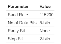
Designing UART Transmitter. This UART Transmitter will have the same parameters as described below. The UART Transmitter should transmit “Hello123”.
Requirements
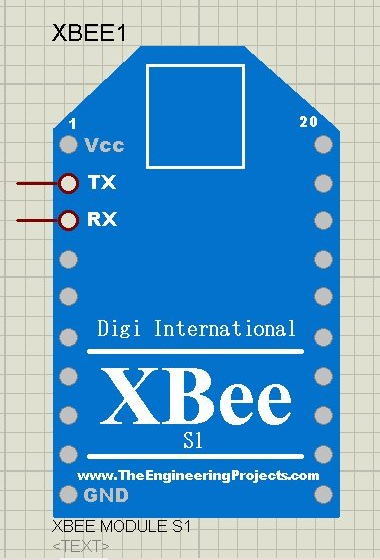
- Xbee s2c Module (2 Qty)
- Jumper wires
- DE0 Nano FPGA
- USB cable A to B
- hterm serial monitor(software)
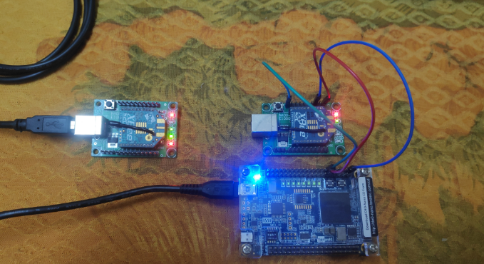
Circuit Diagram
- Connect the RX pin of Xbee to GPIO_00 pin of FPGA
- Connect VCC and GND of Xbee to 3.3v and Gnd of FPGA.
- Connect the second Xbee directly to the Laptop/PC by USB cable A to B
Code
Copy and paste the following code into uart.v or download it from here:
MAIN MODULE
module uart(input clk_50M,//50 MHz clock
output tx //UART transmit output
);

wire temp;//temp count becomes 1 every 11 clock cycles
integer i=0,c=0;//c is clock count
wire clk;//varible for clock used inn accordance to uart baud rate(115200)
reg start; //varable to start with loaded PISO
wire [7:0] tx_op [9:0];//stores data to be transmitted
assign tx_op[0]="H";
assign tx_op[1]="e";
assign tx_op[2]="l";
assign tx_op[3]="l";
assign tx_op[4]="o";
assign tx_op[5]="1";
assign tx_op[6]="2";
assign tx_op[7]="3";
reg initialone ;//variable to get one before 1st character is transmitted
initial begin
start=1;
initialone=1;
end
wire start_or,piso_op;// start_or is for loading piso , piso_op is the output
reg piso_op2;// variable to store delayed piso output
Baudrate_gen clk_gen1(clk_50M,clk);//to convert 50Mhz clock on accordance to 115200 baud rate

div11_ctr ctr1(clk,temp);//to count every 11 cycles

or or1(start_or,start,temp);//for starting with loaded piso and loading piso every time 11 cycles end i.e. new data comes
PISO11 p1(1'b1,1'b1,~start_or, clk,1'b0,    tx_op[i],piso_op);//~start_or
or finalstretchgate(tx,start,piso_op2,initialone);//or gate for getting 1 after end transmission

always @(posedge clk)
begin

if(c==1)  // for measuring 1st clock cycle
initialone=0;
if(temp==1)//for every 11 cycles new data/char
i=i+1;
if(i>8)//transits one after all data is transmitted
start=1;
else
start=0;
c<=c+1;
piso_op2<=piso_op;// delays piso output by 1 cycle
end
endmodule
PISO11 MODULE
module PISO11(
    stopbit2,
    stopbit1,
    shift_notload,
    clk,
    startbit,
    O,
    Out
);

input wire  stopbit2;
input wire  stopbit1;
input wire  shift_notload;
input wire  clk;
input wire  startbit;
input wire  [7:0] O;
output reg  Out;

wire    SYNTHESIZED_WIRE_0;
wire    SYNTHESIZED_WIRE_1;
wire    SYNTHESIZED_WIRE_2;
wire    SYNTHESIZED_WIRE_3;
wire    SYNTHESIZED_WIRE_4
wire    SYNTHESIZED_WIRE_5;
wire    SYNTHESIZED_WIRE_6;
wire    SYNTHESIZED_WIRE_7;
reg DFF_inst15;
reg DFF_inst9;
reg DFF_inst10;
wire    SYNTHESIZED_WIRE_40;
wire    SYNTHESIZED_WIRE_9;
wire    SYNTHESIZED_WIRE_10;
wire    SYNTHESIZED_WIRE_12;
wire    SYNTHESIZED_WIRE_13;
wire    SYNTHESIZED_WIRE_15;
wire    SYNTHESIZED_WIRE_16;
reg DFF_inst11;
wire    SYNTHESIZED_WIRE_18;
wire    SYNTHESIZED_WIRE_19;
reg DFF_inst12;
wire    SYNTHESIZED_WIRE_21;
wire    SYNTHESIZED_WIRE_22;
reg DFF_inst13;
wire    SYNTHESIZED_WIRE_24;
wire    SYNTHESIZED_WIRE_25;
reg DFF_inst16;
wire    SYNTHESIZED_WIRE_27;
wire    SYNTHESIZED_WIRE_28;
reg DFF_inst17;
wire    SYNTHESIZED_WIRE_30;
wire    SYNTHESIZED_WIRE_31;
reg DFF_inst45;
wire    SYNTHESIZED_WIRE_33;
wire    SYNTHESIZED_WIRE_34;
wire    SYNTHESIZED_WIRE_35;
reg DFF_inst49;
wire    SYNTHESIZED_WIRE_37;
wire    SYNTHESIZED_WIRE_38;
wire    SYNTHESIZED_WIRE_39;


assign  SYNTHESIZED_WIRE_40 =  ~shift_notload;

always@(posedge clk)
begin
    begin
    DFF_inst10 <= SYNTHESIZED_WIRE_0;
    end
end

always@(posedge clk)
begin
    begin
    DFF_inst11 <= SYNTHESIZED_WIRE_1;
    end
end

always@(posedge clk)
begin
    begin
    DFF_inst12 <= SYNTHESIZED_WIRE_2;
    end
end

always@(posedge clk)

begin
    begin
    DFF_inst13 <= SYNTHESIZED_WIRE_3;
    end
end

always@(posedge clk)
begin
    begin
    Out <= SYNTHESIZED_WIRE_4;
    end
end

always@(posedge clk)
begin
    begin
    DFF_inst15 <= SYNTHESIZED_WIRE_5;
    end
end

always@(posedge clk)
begin
    begin
    DFF_inst16 <= SYNTHESIZED_WIRE_6;
    end
end

always@(posedge clk)
begin
    begin
    DFF_inst17 <= SYNTHESIZED_WIRE_7;
    end
end

assign  SYNTHESIZED_WIRE_9 = shift_notload & DFF_inst15;
assign  SYNTHESIZED_WIRE_12 = shift_notload & DFF_inst9;
assign  SYNTHESIZED_WIRE_15 = shift_notload & DFF_inst10;
assign  SYNTHESIZED_WIRE_10 = O[4] & SYNTHESIZED_WIRE_40;
assign  SYNTHESIZED_WIRE_39 = SYNTHESIZED_WIRE_9 | SYNTHESIZED_WIRE_10;
assign  SYNTHESIZED_WIRE_13 = O[3] & SYNTHESIZED_WIRE_40;
assign  SYNTHESIZED_WIRE_0 = SYNTHESIZED_WIRE_12 | SYNTHESIZED_WIRE_13;
assign  SYNTHESIZED_WIRE_16 = O[2] & SYNTHESIZED_WIRE_40;
assign  SYNTHESIZED_WIRE_1 = SYNTHESIZED_WIRE_15 | SYNTHESIZED_WIRE_16;
assign  SYNTHESIZED_WIRE_18 = shift_notload & DFF_inst11;
assign  SYNTHESIZED_WIRE_19 = O[1] & SYNTHESIZED_WIRE_40;
assign  SYNTHESIZED_WIRE_2 = SYNTHESIZED_WIRE_18 | SYNTHESIZED_WIRE_19;
assign  SYNTHESIZED_WIRE_21 = shift_notload & DFF_inst12;
assign  SYNTHESIZED_WIRE_22 = O[0] & SYNTHESIZED_WIRE_40;
assign  SYNTHESIZED_WIRE_3 = SYNTHESIZED_WIRE_21 | SYNTHESIZED_WIRE_22;
assign  SYNTHESIZED_WIRE_24 = shift_notload & DFF_inst13;
assign  SYNTHESIZED_WIRE_25 = startbit & SYNTHESIZED_WIRE_40;
assign  SYNTHESIZED_WIRE_4 = SYNTHESIZED_WIRE_24 | SYNTHESIZED_WIRE_25;
assign  SYNTHESIZED_WIRE_27 = shift_notload & DFF_inst16;
assign  SYNTHESIZED_WIRE_28 = O[5] & SYNTHESIZED_WIRE_40;
assign  SYNTHESIZED_WIRE_5 = SYNTHESIZED_WIRE_27 | SYNTHESIZED_WIRE_28;
assign  SYNTHESIZED_WIRE_30 = shift_notload & DFF_inst17;
assign  SYNTHESIZED_WIRE_31 = O[6] & SYNTHESIZED_WIRE_40;
assign  SYNTHESIZED_WIRE_6 = SYNTHESIZED_WIRE_30 | SYNTHESIZED_WIRE_31;
assign  SYNTHESIZED_WIRE_33 = shift_notload & DFF_inst45;
assign  SYNTHESIZED_WIRE_34 = O[7] & SYNTHESIZED_WIRE_40;
assign  SYNTHESIZED_WIRE_7 = SYNTHESIZED_WIRE_33 | SYNTHESIZED_WIRE_34;

always@(posedge clk)
begin
    begin
    DFF_inst45 <= SYNTHESIZED_WIRE_35;
    end
end

assign  SYNTHESIZED_WIRE_37 = shift_notload & DFF_inst49;

assign  SYNTHESIZED_WIRE_38 = stopbit1 & SYNTHESIZED_WIRE_40;

assign  SYNTHESIZED_WIRE_35 = SYNTHESIZED_WIRE_37 | SYNTHESIZED_WIRE_38;

always@(posedge clk)
begin
    begin
    DFF_inst49 <= stopbit2;
    end
end

always@(posedge clk)
begin
    begin
    DFF_inst9 <= SYNTHESIZED_WIRE_39;
    end
end
endmodule
BAUDRATE_GEN MODULE
module Baudrate_gen(clk,clk_OP);
input clk;
output reg clk_OP=1;
integer counter=0;

always @(posedge clk)
begin

    if(counter == 216)
    begin
        clk_OP = ~clk_OP;
        counter<=0;
    end
    else
    counter<=counter+1;
end
endmodule
DIV11_CTR MODULE
module div11_ctr(input clk, output reg tc);
integer counter=0;
initial
tc=1;//possible errors as it executes every time and starts at tc=0 every time
always @(posedge clk)
begin
if(counter==10)
begin
counter<=0;
tc=1;
end
else
begin
counter <= counter +1;
tc=0;
end
end
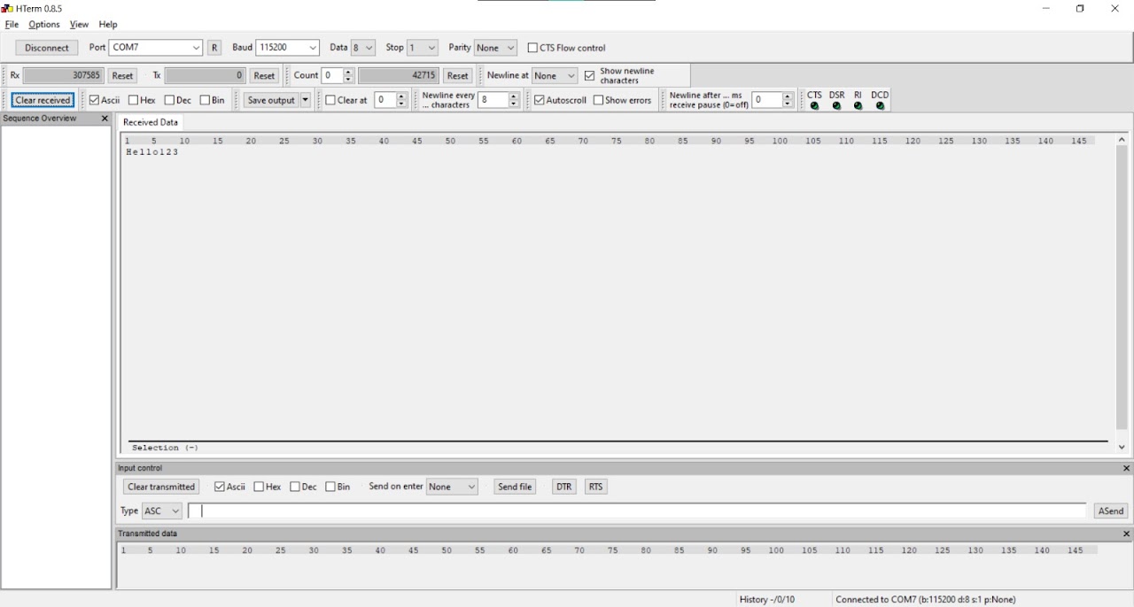
endmoduleOutput
Hello123 will be printed in the hterm serial monitor.
Conclusion
In conclusion, interfacing a UART with an FPGA is a common and manageable task. The FPGA can be programmed to handle the UART's serial communication, data formatting, clocking, and protocol-specific features, allowing for seamless integration into larger system designs.