Getting started with Quartus
Creating a new project
To create a new project in Quartus Lite follow the below steps:
Note: Follow the steps carefully as once the project is created some settings cannot be changed.
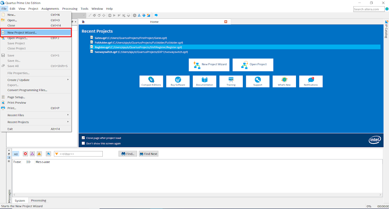
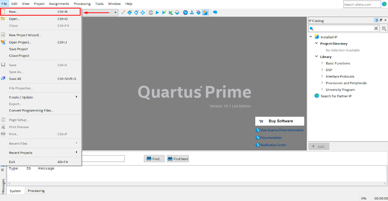
Click File → New Project Wizard to quickly setup a new project. Alternatively, New Project Wizard can be opened from the Home Tab that is seen when Quartus is opened.
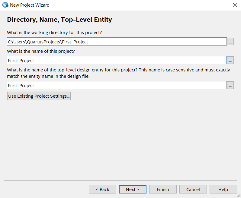
Click Next on the Dialog Box and select the Directory in which the project is to be saved. Give the Project Name and Click on Next.
Note: In below image the directory chosen is “C:\Users\QuartusProjects\First_Project”, but you must create a different folder named AND_GATE anywhere on your local machine and choose this directory (Do not create this folder in C drive). Also, name the project as AND_GATE. Top Level Module will be default i.e. AND_GATE
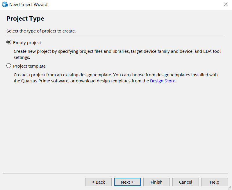
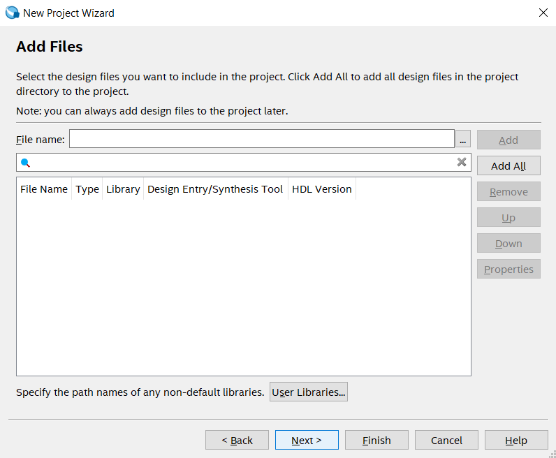
Click on Empty Project. Selecting this option will allow us to manually specify the additional files and libraries, device family and EDA(Electronic Design Automation) tool setting.
In Add Files section, click on Next. For this project we don’t require any additional files, so now we can continue without adding any file in our project.
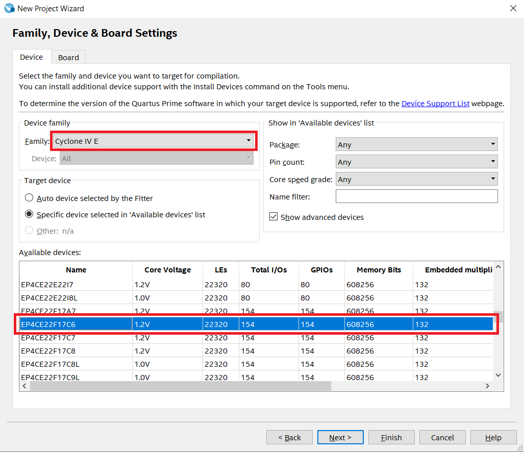
Choose the FPGA Device that is being used. Click on Family and choose the Cyclone IV E. Select "EP4CE22F17C6" from the Available Device. We can also search the device using the options provided in right side of the window
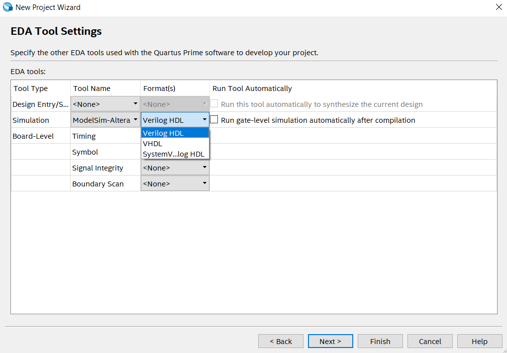
Select the tools used in this project. For Simulation tool name choose ModelSim-Altera. Also, choose simulation format as Verilog HDL.
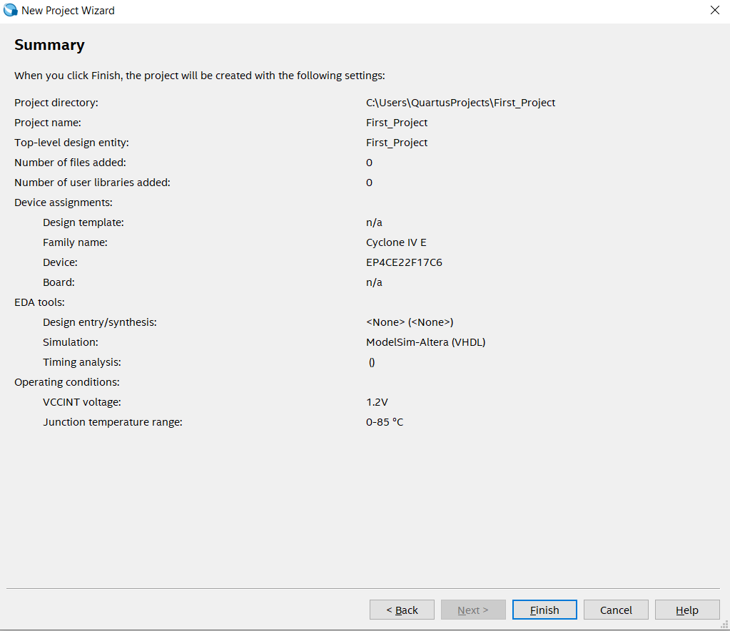
Review the summary, you can change the entries by Clicking on Back as we can not change these setting later in our project and make sure all the entries are correct. Click on Finish to successfully create a New Project.
Creating new files in the project
In the previous steps, we created a directory and selected device families and simulation tool to set up a Quartus project, which tells the tool about the board we are using. We now need to add some actual circuitry to this project. We will create a simple design of an AND gate and this design will have two data inputs A and B and a single output C.
Follow the below steps to add necessary file in our project:
Click on File → New
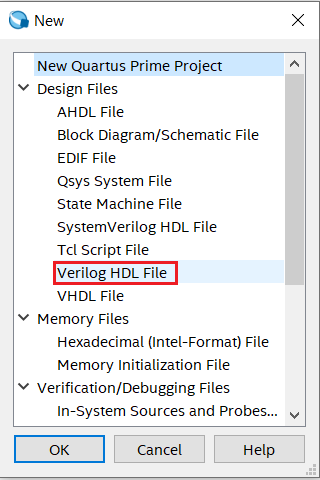
Select Verilog HDL.
Write down the below code in the newly created file. Also note that Verilog HDL is case sensitive.
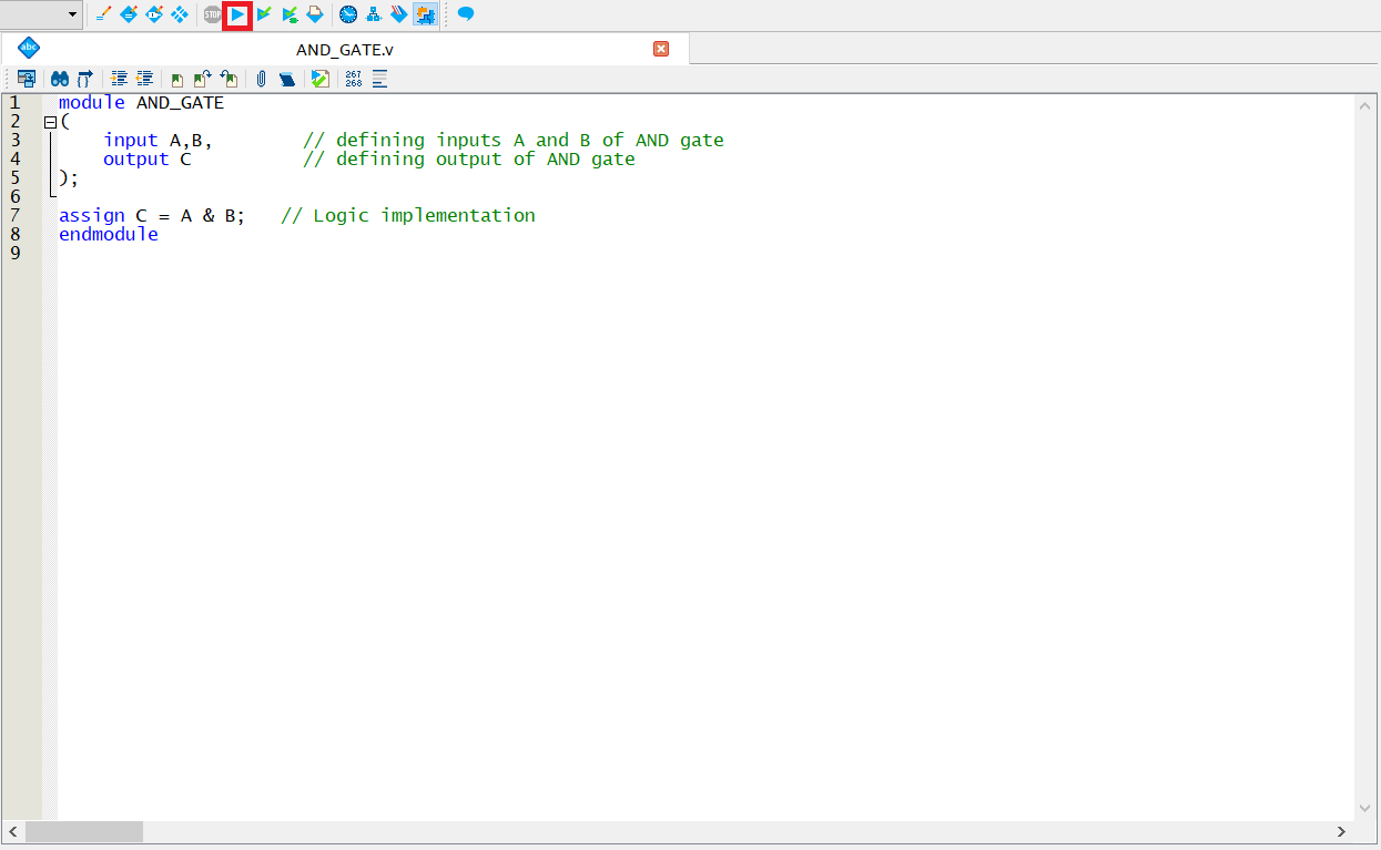
Verilog Code for AND gate
module AND_GATE (
    input  A,
    B,  // defining inputs A and B of AND gate
    output C   // defining output of AND gate
);

  assign C = A & B;  // Logic implementation
endmodule
After completing the code click on File → Save As.
Enter the name of file (it should be same as module name i.e. AND_GATE), enter correct file extension. For Verilog HDL file extension is .v and then Click on Save.
Compiling the Project Files
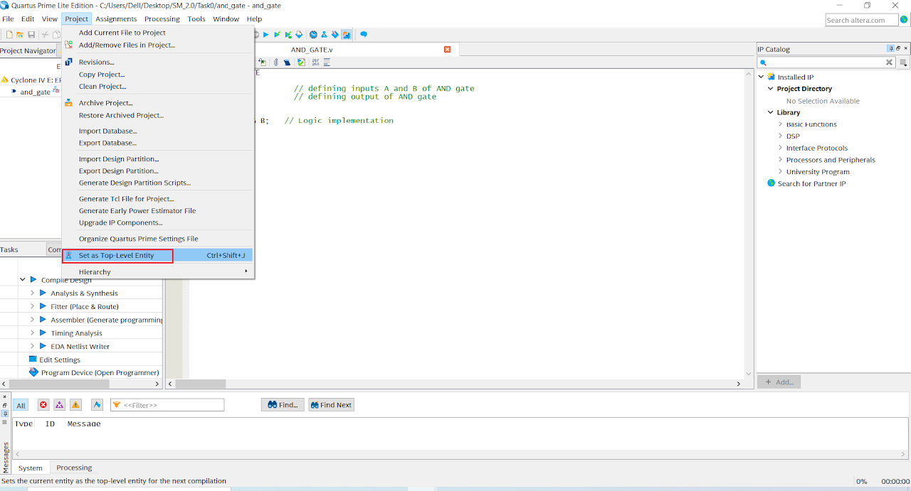
To compile the file, the file must be the top-level enity of the project. We can assign the AND_GATE.v file as top-level entity by Project → Set as Top-Level Entity option in toolbar.
Generate synthesis or final compilation results by running the following commands: Click Start Compilation shown in the figure below (red box) to generate final compilation results.
You should obtain a green tick on the Task Bar for successful compilation.
Verification of Output of AND Gate
You can perform functional and timing simulation of design by using simulation tools.
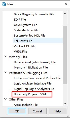
- Click on File→New→University Program VWF.
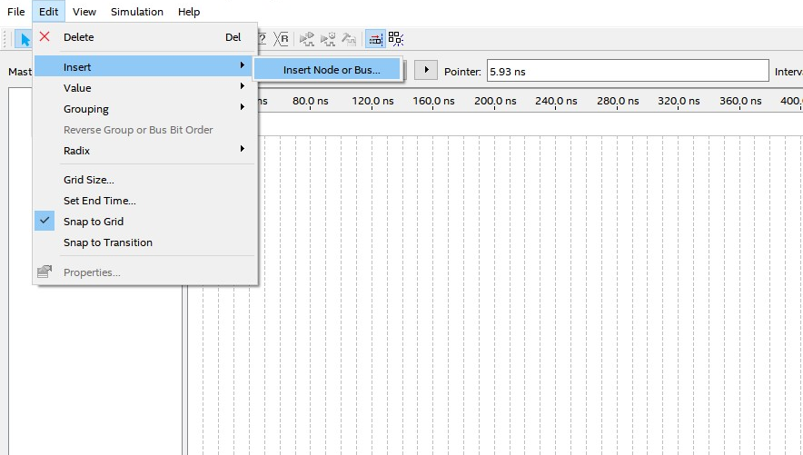
- In the New window, Go to Edit→Insert→Insert Node or Bus.
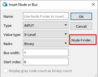
- Click on Node Finder, in the New Window, Click on List.
- Click on List option. Then click on the highlighted button to add all the Nodes. Now Click on OK and then OK again.
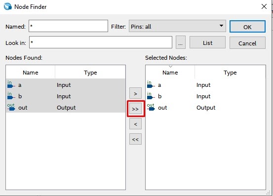
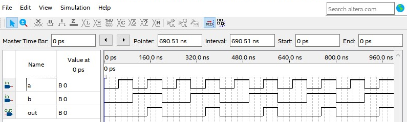
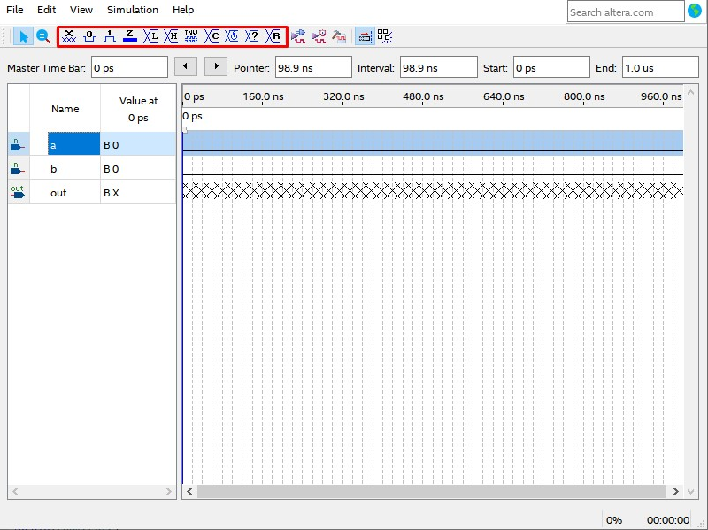
Note : For our design a = A, b = B and out = C.
- Choose Input A and specify its value by choosing any of the options that are highlighted .
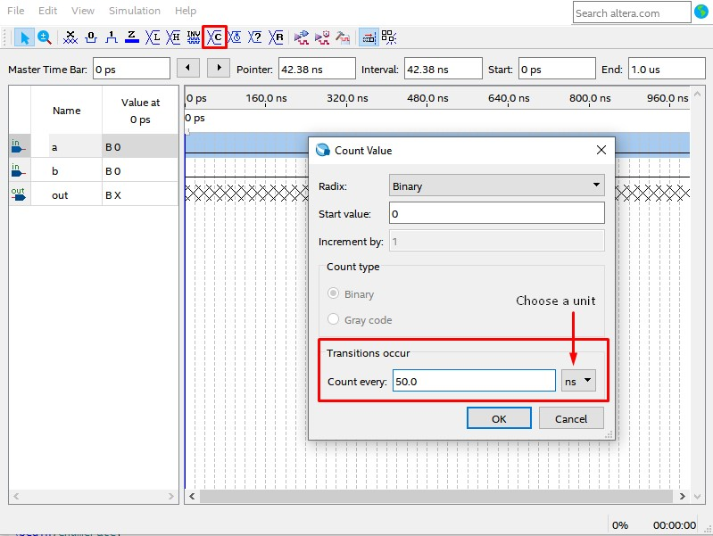
- For example, to give the Clock pulse to A input, select the node, then Click on the Count Value button highlighted at the top in the below figure, and then specify the Clock Pulse of frequency 50ns.
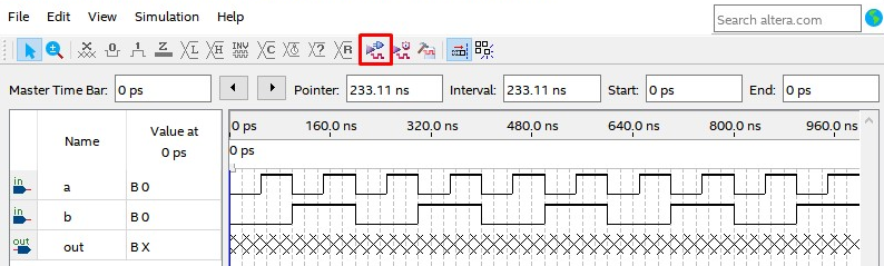
- Similarly, specify the input pattern for input B with Clock Pulse of frequency 100ns and then Click on the Simulate Icon. If a save prompt appears, then save the file. Do not change the file name and also do not change its location. By default file name will be Waveform.vwf and it will be stored by default in the project folder. Once the simulation process completes, the waveform will be displayed. This is the waveform before the simulation starts.
This is the waveform after the simulation ends.