Interfacing LED with DE0 Nano FPGA
Introduction
Problem statement
Blinking an LED on FPGA DE0 Nano.
Requirements
FPGA DE0 Nano.
Working
Code
Copy and paste the following code into blinkled.v or download it from here:
module blinkled (input  clk, output out);
  reg [31:0] counter;
  reg LED;

  initial begin
    LED = 1'b0;
    counter = 32'b0;
  end

  always @(posedge clk) begin
    if (counter < 25000000) counter <= counter + 1'b1;
    else begin
      LED <= ~LED;
      counter <= 32'b0;
    end
  end

  assign out = LED;

endmodule
Navigate to Following:
Assignment --> Pin-Planner
or you can directly get the pin-planner shortcut as shown below in quartus interface:

or press Ctrl+Shift+N.
Following window will appear:
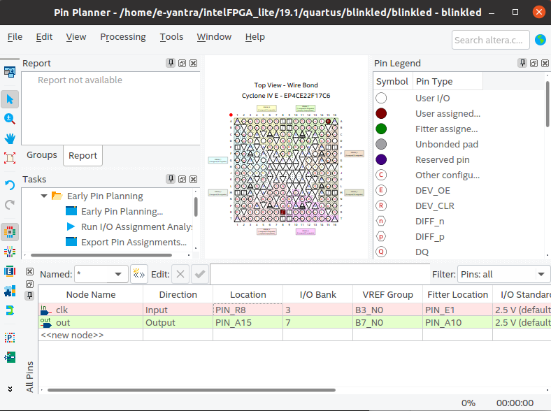
Enter the location for the node names as mentioned below.
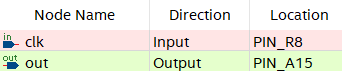
- clk assigned to PIN_R8.
- out assigned to PIN_A15.
For Hardware Seup refer DE0 Nano Manual
After typing in the location pin of Input, close the window.
Next step is to compile it again by using the start compilation button on the menu bar.
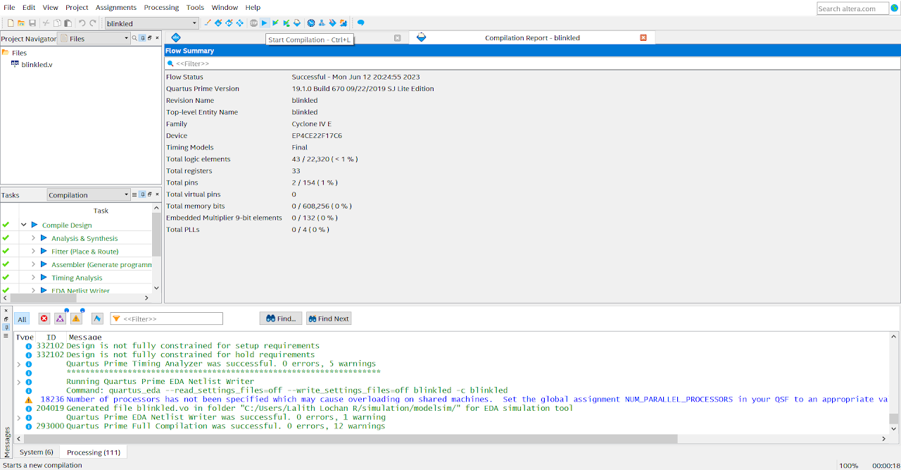
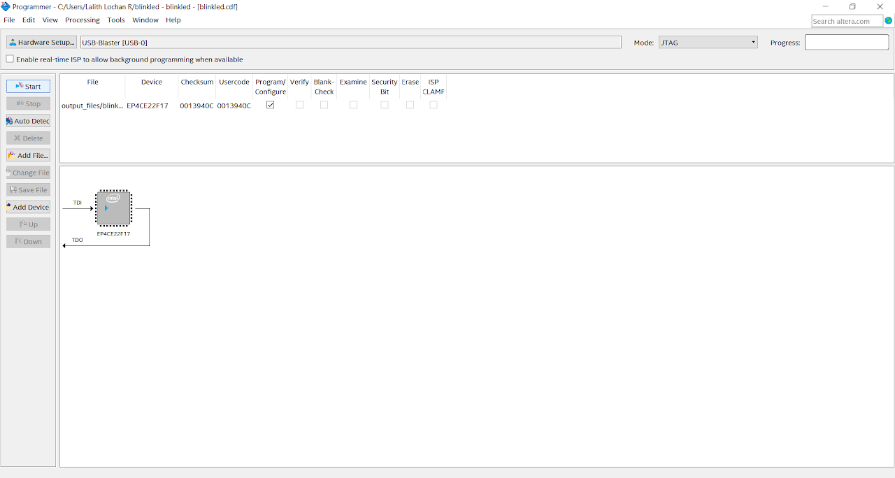
After successful compilation click on the programmer button on menu bar.
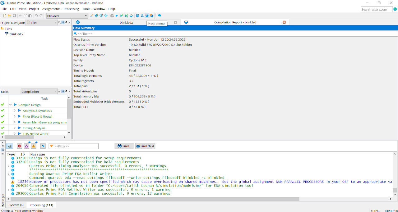
You will be taken to a new window as shown below.
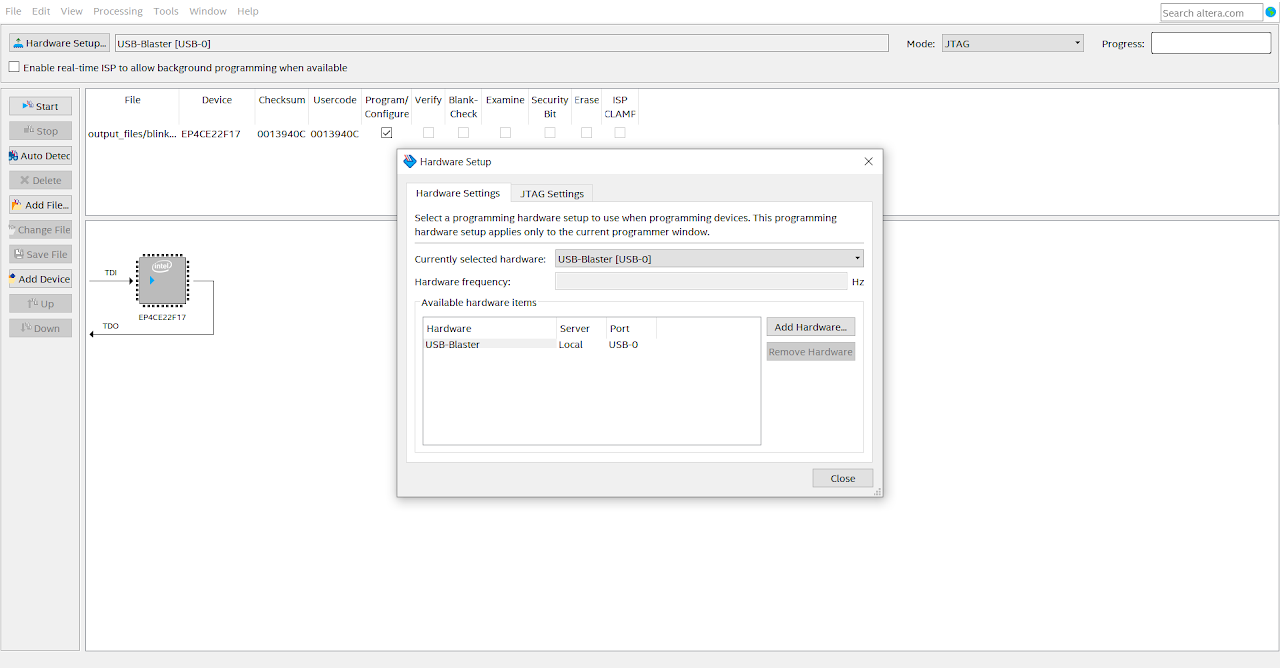
Setup USB-Blaster:
for Windows user - click here. for Linux user do the following:
create a file named "51-usbblaster.rules" in "/etc/udev/rules.d/" using following command:
sudo touch /etc/udev/rules.d/51-usbblaster.rulesAdd following lines in file:
# USB Blaster

SUBSYSTEM=="usb", ENV{DEVTYPE}=="usb_device", ATTR{idVendor}=="09fb", ATTR{idProduct}=="6001", MODE="0666", NAME="bus/usb/$env{BUSNUM}/$env{DEVNUM}", RUN+="/bin/chmod 0666 %c"
SUBSYSTEM=="usb", ENV{DEVTYPE}=="usb_device", ATTR{idVendor}=="09fb", ATTR{idProduct}=="6002", MODE="0666", NAME="bus/usb/$env{BUSNUM}/$env{DEVNUM}", RUN+="/bin/chmod 0666 %c"
SUBSYSTEM=="usb", ENV{DEVTYPE}=="usb_device", ATTR{idVendor}=="09fb", ATTR{idProduct}=="6003", MODE="0666", NAME="bus/usb/$env{BUSNUM}/$env{DEVNUM}", RUN+="/bin/chmod 0666 %c"

# USB Blaster II

SUBSYSTEM=="usb", ENV{DEVTYPE}=="usb_device", ATTR{idVendor}=="09fb", ATTR{idProduct}=="6010", MODE="0666", NAME="bus/usb/$env{BUSNUM}/$env{DEVNUM}", RUN+="/bin/chmod 0666 %c"
SUBSYSTEM=="usb", ENV{DEVTYPE}=="usb_device", ATTR{idVendor}=="09fb", ATTR{idProduct}=="6810", MODE="0666", NAME="bus/usb/$env{BUSNUM}/$env{DEVNUM}", RUN+="/bin/chmod 0666 %c"
Create a new file named "usbblaster.rules" in same directory (/etc/udev/rules.d/) and add following content:
Note: Add your laptop's username in GROUP in place of <user-name>.
ATTR{idVendor}=="09fb", ATTR{idProduct}=="6001", GROUP="<user-name>"restart udev using following command:
sudo service udev restartAfter setting up USB-Blaster, Click on Hardware Setup and Select USB-Blaster in currently selected hardware as shown below and close window.
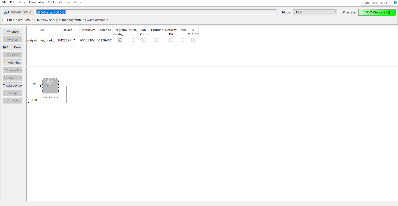
Click on the start button and you should see the progress as 100% (Successful) as shown below.
Output
This code implements a simple blinking of inbuilt LED functionality on an FPGA board. The LED(LED[0]) turns on and off periodically based on the clock signal, with a toggle rate controlled by the counter value.
Conclusion
From this Verilog code for interfacing an LED in the DE0 Nano FPGA, we learned several key concepts. Firstly, we saw how to initialize and control signals using Verilog syntax, including the input (clk) and output (out) ports. We observed the use of a clock signal to synchronize the blinking of the LED. The counter was used to determine the toggle rate of the LED, allowing for a specific blinking frequency. We also witnessed the usage of if-else conditions to handle the toggle action. Lastly, we gained insights into assigning the LED output value to the designated output port using the assign statement. Overall, this code demonstrated the fundamentals of interfacing an LED with an FPGA using Verilog, showcasing how to control the LED's blinking behavior based on the clock signal.