P89V51RD2 Development Board
About the board
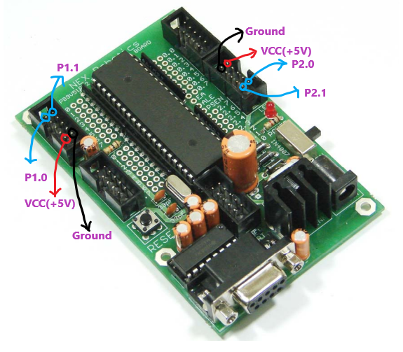
P89V51RD2 Development Board is a low cost development board which have all the basic components needed for gaining a headstart on your first 8051 microcontroller projects. It is made from double sided PTH PCB board to provide extra strength to the connector joints for increased reliability. Board can work on 7 to 15V AC or DC supply. It has built-in reverse polarity protection. 7805 voltage regulator has heat sink for heat dissipation so that it can supply 1Amp current continuously without getting over heated. It has switches for reset and power. It also has RS232 interface with DB9 female connector based on MAX232. All the ports are connected to standard 10-pin FRC connectors. Open pads for connecting microcontroller’s pins to external devices are also provided. It can be programmed using Flash Magic programming utility of NXP’s own programming utility via serial port.
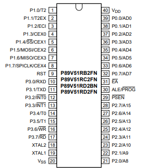
Features of 8051 microcontroller
- 8-bit microcontrollers with 80C51 core
- 64 kB of on-chip Flash program memory with ISP (In-System Programming) and IAP (In-Application Programming)
- Supports 12-clock (default) or 6-clock mode selection via software or ISP
- SPI (Serial Peripheral Interface) and enhanced UART
- PCA (Programmable Counter Array) with PWM and Capture/Compare functions
- Four 8-bit I/O ports with three high-current Port 1 pins (16 mA each)
- Three 16-bit timers/counters
- Programmable Watchdog timer (WDT)
- Eight interrupt sources with four priority levels
- Second DPTR register
- Low EMI mode (ALE inhibit)
- TTL- and CMOS-compatible logic levels
- Brown-out detection
- Low power modes
Refer following links for more information about the Development board: