Interfacing Line Sensor with DE0 Nano FPGA
Introduction:
Line sensors are used for sensing white line on dark surface or black line on light surface. These line sensor boards have One, Three, Five or Seven line sensors connected together. These sensors working together can follow any curved or zigzag path. Because of multiple sensors it can even detect nodes and move on the maze of white or black lines. Line sensor consists of high intensity red LED for illumination and directional photo transistor for line sensing. Phototransistor consists of a photo transistor and convex lense. Because of precise alignment between lense and photo transistor it has very narrow viewing angle of 5 degrees. This makes this line sensor highly immune to ambient light. This sensor gives 0.18 volts on bright surface and gives 2.2V or more on the dark surface. Its output is analog in nature.
Problem Statement
Interfacing Line Sensor with DE0 Nano FPGA Board.
Requirements
- DE0 Nano Board
- Breadboard
- Line sensor
- Potentiometer(10k)
- Jumper wires
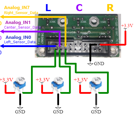
Circuit Diagram
- Assign clk to R8 in Pin Planner.
- Assign a to PIN_A15, b to PIN_A13, c to PIN_B13
- Assign adc_sck to PIN_B14
- Assign adc_cs_n to PIN_A10
- Assign din to PIN_B10
- Assign dout to PIN_A9
Code
Copy and paste the following code into Main.c or download it from here:
module adc_control(

    input  clk,              //50 MHz clock
    input  dout,                //digital output from ADC128S022 (serial 12-bit)
    output adc_cs_n,            //ADC128S022 Chip Select
    output reg din,             //Ch. address input to ADC128S022 (serial)
    output adc_sck,         //2.5 MHz ADC clock
    output a,b,c);

integer count;
reg cs;
reg cs1;
integer count2;
reg countt;
integer countadc1;
reg adc_sck1;
integer incount;
integer countadc;
integer data_frame1;
integer count3;
integer count4;
integer count5;
integer count6;
integer count7;
integer count8;
integer d_out_ch71;
integer d_out_ch61;
integer d_out_ch51;
reg din1;
reg [0:11] temp0;
reg [0:11] temp1;
reg [0:11] temp2;
wire [11:0]d_out_ch5;   //12-bit output of ch. 5 (parallel)
wire [11:0]d_out_ch6;   //12-bit output of ch. 6 (parallel)
wire    [11:0]d_out_ch7;
wire [1:0]data_frame    ;

initial
begin
count=0;
count2=0;
countadc1=1;
count3=0;
count4=0;
count5=0;
count6=0;
count7=0;
count8=0;
incount=1;
countt=0;
countadc=0;
din1=0;
cs=1;
cs1=1;
adc_sck1=0;
data_frame1=0;
d_out_ch71=0;
d_out_ch61=0;
d_out_ch51=0;
temp0=12'b0;
temp1=12'b0;
temp2=12'b0;

end

//This and the proceeding always blocks are used to generate CS signal after 16 clock cycles of acc_sck
always@(posedge adc_sck)
begin
    countadc<=countadc+1;
    if(countadc==16)
    begin
        cs<=adc_sck;
        countadc<=1;
    end
    if(countadc==1)
        cs<=0;
end

always@(negedge adc_sck)
begin
    countadc1<=countadc1+1;
    if(countadc1==16)
    begin
        cs1<=1;
        countadc1<=1;
    end
    if(countadc1==1)
        cs1<=0;

end
//this always block generates adc_sck i.e,2.5MhHz clock for ADC

always@(negedge clk_50)
begin
    count<=count+4'd1;
    if(count==320)
        count<=1;
    count2<=count2+1;
    if(count2==10)
    begin
        adc_sck1=~adc_sck1;
        count2<=1;
    end
end

always@(negedge adc_sck)
begin
    case(data_frame)//this case statement gathers the serial to parral converted digital 12 bit output on to the correct d_cot channel
    2'b00:
        d_out_ch61=temp2;
    2'b01:
        d_out_ch71=temp0;
    2'b10:
        d_out_ch51=temp1;
    endcase
end
always@(negedge adc_sck)
begin
    incount<=incount+1;
    if(incount==16)
    begin                     //updation of dataframe happens here

        data_frame1=data_frame1+1;
        if(data_frame1==2'b11)
            data_frame1=0;
        incount<=1;
    end
    case(data_frame)//output of the address of the analog pin from which analog to digital conversion should be happening is given here
    2'b00 :
    begin
        count3<=count3+1;

        case(count3)
        3'b000 : din = 0;
        3'b001 : din = 0;
        3'b010 :
        begin
            din = 0;
            count3<=0;
        end
        default : din = 0;
        endcase
    end
    2'b01 :
    begin
    count4<=count4+1;

    case(count4)
    3'b000 : din = 0;
    3'b001 : din = 0;
    3'b010 :
    begin
        din = 1;
        end
        5'b01111:
        begin
            din=1;
            count4<=0;
        end
        default : din = 0;
        endcase
    end
    2'b10 :
        begin
        count5<=count5+1;
        case(count5)
        3'b000 : din = 1;
        3'b001 : din = 1;
        3'b010 :
        begin
            din = 1;
            count5<=0;
        end
        default : din = 1;
        endcase
    end
    endcase
end

//assignment of all the register values to wires

assign adc_cs_n = cs & cs1;
assign adc_sck = adc_sck1;
assign data_frame=data_frame1;

assign d_out_ch7 = d_out_ch71;
assign d_out_ch6 = d_out_ch61;
assign d_out_ch5 = d_out_ch51;

always@(posedge adc_sck)//collecting the digital output of ADC from each clock pulse serially and converting it to parallel
begin
    case(data_frame) //dataframe start
        2'b00 :
        begin
        count6<=count6+1;
        case(count6)
            3'b100 : temp0[0]<=dout;
            3'b101 : temp0[1]<=dout;
            3'b110 : temp0[2]<=dout;
            4'b111 : temp0[3]<=dout;
            4'b1000 :temp0[4]<=dout;
            4'b1001 :temp0[5]<=dout;
            4'b1010 :temp0[6]<=dout;
            4'b1011 :temp0[7]<=dout;
            4'b1100 :temp0[8]<=dout;
            4'b1101 :temp0[9]<=dout;
            4'b1110 :temp0[10]<=dout;
            4'b1111 :
            begin
            temp0[11]<=dout;
            count6<=0;
            end
    endcase
    end
    2'b01 :
    begin

    count7<=count7+1;
        case(count7)

            3'b100 :temp1[0]<=dout;
            3'b101 :temp1[1]<=dout;
            3'b110 :temp1[2]<=dout;
            4'b111 :temp1[3]<=dout;
            4'b1000 :temp1[4]<=dout;
            4'b1001 :temp1[5]<=dout;
            4'b1010 :temp1[6]<=dout;
            4'b1011 :temp1[7]<=dout;
            4'b1100 :temp1[8]<=dout;
            4'b1101 :temp1[9]<=dout;
            4'b1110 :temp1[10]<=dout;
            4'b1111 :
            begin
            temp1[11]<=dout;
            count7<=0;
            end

    endcase
    end
    2'b10 :
    begin
        count8<=count8+1;
        case(count8)
            3'b100 : temp2[0]<=dout;
            3'b101 : temp2[1]<=dout;
            3'b110 : temp2[2]<=dout;
            4'b111 : temp2[3]<=dout;
            4'b1000 :temp2[4]<=dout;
            4'b1001 :temp2[5]<=dout;
            4'b1010 :temp2[6]<=dout;
            4'b1011 :temp2[7]<=dout;
            4'b1100 :temp2[8]<=dout;
            4'b1101 :temp2[9]<=dout;
            4'b1110 :temp2[10]<=dout;
            4'b1111 :
            begin
            temp2[11]<=dout;
            count8<=0;
            end
        endcase
    end
    endcase
end

assign c= (d_out_ch51>12'b100110110100) ? 0:1 ;//cutoff value for right sensor
assign b= (d_out_ch61>12'b100110110100) ? 0:1 ;//cutoff value for middle sensor
assign a= (d_out_ch71>12'b100110110100) ? 0:1 ;//cutoff value for left sensor
//all these values should be calibrated

endmodule
Output
when the left sensor faces a black line then LED0 turns off, if the left sensor faces a white line LED0 turns on. The same outputs are for the middle and right sensors.
Conclusion
interfacing a line sensor with an FPGA enables real-time and accurate line detection, leveraging the FPGA's parallel processing capabilities and flexibility. The FPGA can process the sensor data, extract relevant information, and provide control signals for precise navigation or control actions. This integration is beneficial for a wide range of applications, including robotics, automation, and computer vision systems that rely on line detection and tracking.